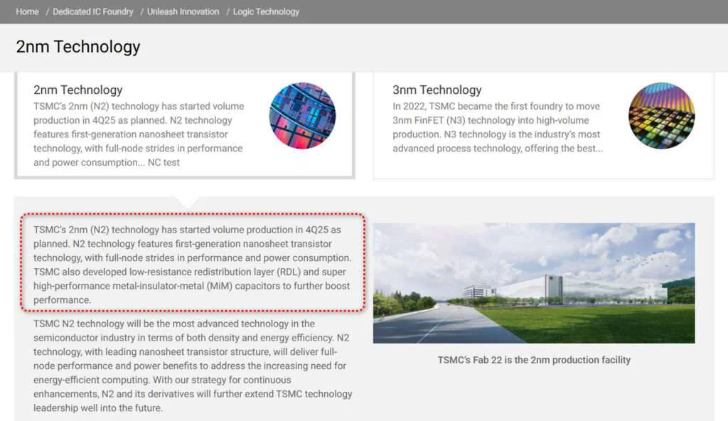
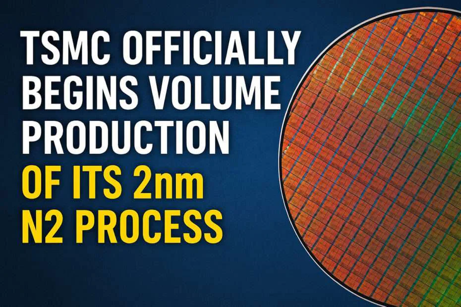
After years of development, TSMC has now crossed a crucial threshold. The company confirmed that volume production of its 2-nanometer process quietly began in the fourth quarter of 2025, keeping its ambitious timeline intact.

For more than a decade, FinFETs carried TSMC through successive process nodes. With N2, that era comes to an end. The company is adopting Gate-All-Around nanosheet transistors, a design that wraps the gate around stacked horizontal channels, tightening control over current and enabling smaller, more efficient chips without giving up speed.
TSMC CEO C.C. Wei said during an October earnings call that N2 remains on schedule for volume production later in the quarter, with yields meeting expectations.
In addition to GAA transistors, the N2 platform includes several other technical improvements. These include Super-High-Performance Metal-Insulator-Metal (SHPMIM) capacitors in the power delivery network, which TSMC says provide more than twice the capacitance density of earlier designs while reducing resistance by half, improving power stability and efficiency.
Relative to TSMC’s N3E process, N2 is expected to provide 10-15% higher performance at the same power, or reduce power consumption by 25-30% at comparable performance. Logic-only designs are also projected to see density gains of up to 20%.
TSMC initiated high-volume manufacturing at Fab 22 in Kaohsiung rather than at Fab 20 in Hsinchu, which is closely tied to R&D. Fab 20 is expected to join the production effort later. The initial rollout also spans a wider range of end markets, covering smartphones and high-performance computing applications, including AI accelerators.
Demand is driving an aggressive capacity expansion. “We expect a faster ramp in 2026, fueled by both smartphone and HPC AI applications,” Wei noted. The company is preparing both N2-capable fabs in parallel and plans to scale output through 2026 to accommodate future process variants.
The company plans to launch N2P, a faster version of the node, in the second half of 2026, and will also debut A16, which brings its own Super Power Rail backside power delivery technology into the mix.
Wei described A16 as a better fit for HPC chips with complex signal paths and heavy power demands. By moving power wiring to the back of the wafer, the technology is designed to squeeze out more performance and density for advanced AI and HPC processors. TSMC still expects both N2P and A16 to reach volume production in late 2026.
Maybe you would like other interesting articles?

