
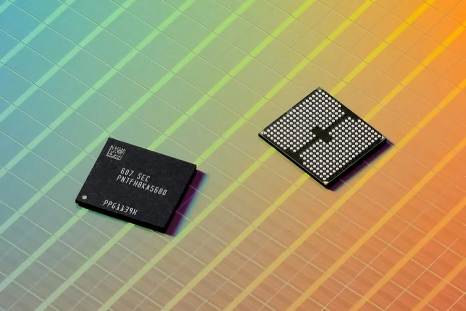
At the Future of Memory and Storage 2026 event in Santa Clara, Samsung Electronics gave a closer look at the memory technologies it believes will power the next generation of AI. The company showcased plans for V-NAND with more than 400 layers, a design that places high-bandwidth memory directly on AI chips, and a new low-latency NAND solution built for edge AI.
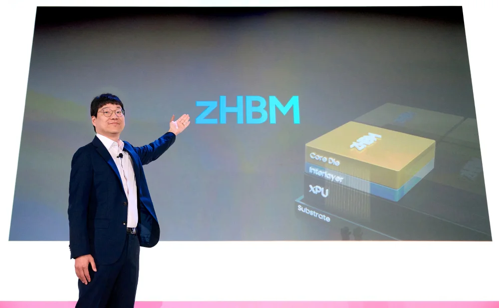
A key part of Samsung’s roadmap is zHBM, a concept that changes the placement of high-bandwidth memory. Instead of positioning HBM beside the AI processor, the memory stack is bonded directly to the top of the compute die. Samsung says this layout reduces data travel distance, helping improve both bandwidth and power efficiency during AI training and inference.
Samsung estimates that systems built around its next-generation zHBM interface could deliver about eight times the performance of HBM5. The company also says wafer bonding could increase memory density by more than 10 times, triple energy efficiency, and cut thermal resistance by over 50 percent. Those thermal improvements, Samsung added, would help make high-capacity AI systems more stable and easier to cool.
The zHBM design is also intended to make AI hardware more adaptable. It allows customer-specific IP to be added between the memory stack and the AI accelerator, where it can be used to increase memory capacity or include logic optimized for different AI workloads.
V10 BV-NAND: first bonding V-NAND with over 400 layers
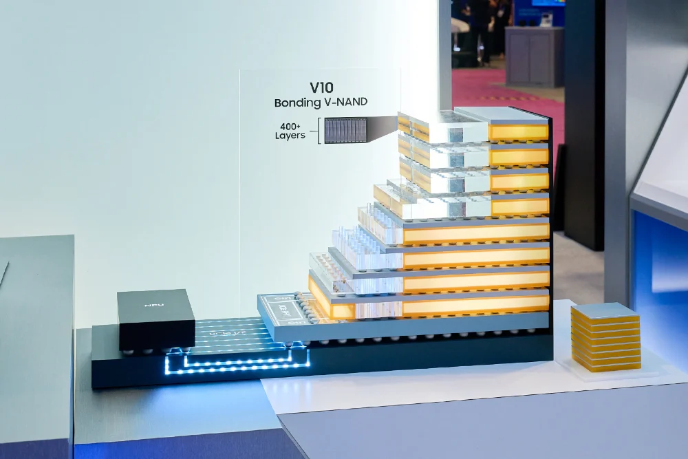
Among all the concepts Samsung showcased, V10 BV-NAND was the product closest to becoming reality. The company says it’s the industry’s first Bonding V-NAND design, using wafer bonding to stack memory cells and pack more than 400 layers into a single chip.
According to Samsung, the higher layer count helps V10 BV-NAND increase storage density and performance while lowering power consumption. The company says the new architecture delivers about 58 percent higher memory density than V9, along with faster read, write, and input/output performance. It is designed for high-capacity NAND in next-generation AI systems.
Samsung also outlined zNAND-O, a new storage technology aimed at edge AI systems that demand low power consumption and rapid response times. Based on the company’s V-NAND architecture, zNAND-O is being developed in four- and eight-layer variants. Samsung says it will offer a combination of high storage density, faster I/O performance, and low latency, filling the gap between conventional NAND storage and specialized memory designed for AI inference.
Maybe you’d like some other interesting articles?